Engineering 100-950
Lab 7: Designing a PCB using KiCad
Contents
Introduction
In this lab, you will be designing a PCB using KiCad, an industry-standard PCB design tool. It’s crucial to focus on creating a high-quality design, as changes cannot be made to a PCB after the design is sent off to be manufactured. There is no post-lab for this lab (besides turning in your final design), but you will be reviewing each other’s PCBs. Focus on making sure your design is good, and everything about your board works.
Required KiCad Library:
Final Project Library Folder
Participation
Working at a computer can easily become a one-person activity. It is important to avoid this during the lab. Our goal is for all students in this course to learn the basics of KiCad. When you are working on your PCBs, have at least one person spotting the person at the computer. This will help you share the work that goes into creating the PCB and eliminate mistakes that can render your finished product useless. It is important that no team member works alone, even during office hours.
Lab Timeline
- February 26th, 2026, 3:00pm: Initial PCB design submission.
- February 26th, 2026, 5:00pm: Peer review submissions due.
- February 27th, 2026, 12:00 noon: Final PCB design submission.
KiCad
The walkthrough on creating a schematic and turning the schematic into a PCB is in lab-7-prelab. Make sure you do this before starting the KiCad project.
Broadly, the workflow in KiCad is divided up into three steps: Schematic, PCB, and Design Rule Check. The Schematic step is where you lay out the electrical schematic of your board. Using all the components, you define how they connect to each other, ground, and power. The PCB step is where you make the physical layout of those components on the board. The electrical connections you set up in the schematic are shown for your reference, and you lay them down on your PCB physically as traces. That is, each trace you set corresponds to an electrical connection you outlined in your Schematic. The Design Rule Check step is when the software looks over your work and makes sure you aren’t committing any errors or contradictions. This is inevitably the most frustrating part of using KiCad, because you think you’ve done everything right, and the software is here to tell you that you haven’t. It is important to note that design rule checks do not check whether you laid out your board the way you wanted, they will not notice if you accidentally connected your temperature sensor to your pressure sensor instead of the Arduino (if that is what you did in your schematic). You must double check this yourself. The design rule checks only check if your design rules are violating the physical and electrical laws associated with making a PCB.
Schematic
Background
You begin with an idea. A circuit or device that you’d like to realize in a PCB. The first thing you need to do is tell KiCad the components you’ll be using, and their relationships to one another. Consider the drawing of a self-running astable multivibrator below.
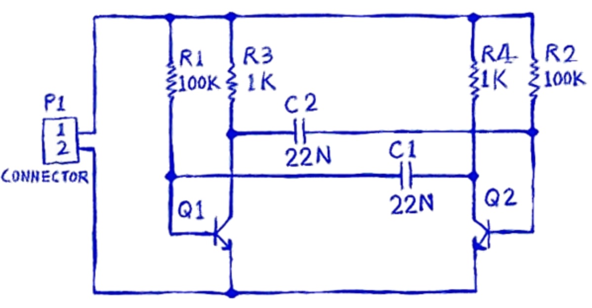
Figure 1: A drawing of a schematic, that pretty closely resembles a schematic you’d make in KiCad.
Figure 2 shows Figure 1 as a KiCad schematic. In KiCad, schematic files use the .kicad_sch extension.
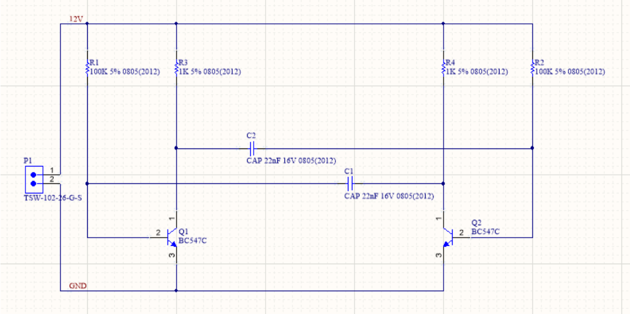
Figure 2: The schematic of an astable multivibrator as displayed through KiCad.
For additional reference, here is the schematic you made following Lab 1:
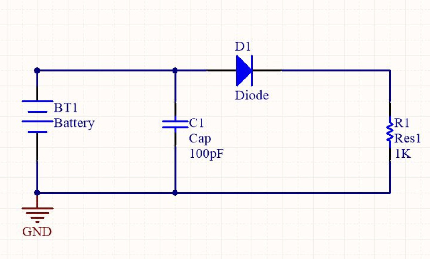
Figure 3: The schematic completed in the Postlab 1 assignment
Note that each component is defined with its own individual symbol. Capacitors, resistors, and transistors (Q1 and Q2), and some connectors (P1) are standardized and thus have pre-loaded symbols in the software, but for most of our components, that is not the case. We have additional libraries custom made by ENGR100 staff with our components pre-loaded, so as we will discuss in the procedure, you can simply drag and drop them into place. Use only the Final Project Library linked above.
Your Schematic Contents
Obviously, the functionality we’re trying to put on a PCB is the ability to record data from your sensor board, so starting your schematic off by adding your full Lab 3, 4, and 5 circuits is a good starting point.
We have made a power board that provides you the LDOs and battery connector. This is included in the provided Final Project Library.
LEDs are also useful when diagnosing software bugs without a computer, telling you if the board is on or off, and also making cool light patterns.
You will also use resistors and capacitors.
Please wire the 5V, 3.3V and battery line to their own LEDs with a 1K resistor on each LED. You are free to add LEDs in other places on your board if you would like!
Footprints of LEDs, resistors and capacitors:
- Capacitors have to be 1206 SMD (surface mount only)
- LEDs have to be LED_THT:LED_D5.0mm (thru-hole)
- Resistors can be 1206 SMD (surface mount) or Resistor_THT:R_Axial_DIN0207_L6.3mm_D2.5mm_P7.62mm_Horizontal (thru-hole)
Some notes:
- As you place sensors on your schematic, change the label on the top of the sensor. Some have a label of ‘’, while others are ‘Temperature’. Give them all unique names that make sense (like TMP36 or Datalog).
- Ground all of your components using a “GND Power Port”
- Connect 5V pins together from the power board with arduino 5V pin (this will power the Arduino) and all other 5V power connections on the 5V powered devices. There should be NO connection to the Vin pin of the Arduino! You could make a 5V Net to make things cleaner.
In summary, your schematic (and the PCB) must have:
- An Arduino Nano Every (voltage input should be through the 5V connector and nothing should be connected to the Vin pin)
- TMP36 or thermister (external temperature) - if using thermister, talk to teaching staff
- BME sensor (humidity, pressure, and temperature)
- Accelerometer
- GPS
- Level shifter
- SD Card writer
- LEDs with resistors from 3.3V, 5.0V, and battery voltage lines to ground
- Any extra sensors you choose to use
- The power daughter board (which includes battery connection, RBF pin, LDOs, and capacitors)
- 0.1 uF (micro-F) capacitors from the input voltage line on the GPS to ground, the SD card input voltage to ground, and the Arduino 5V pin to ground (3 capacitors).
- 0.1 uF (micro-F) capacitors from input line to ground close to TMP36, BME680, and accelerometer (3 more capacitors).
- A voltage divider running off of the battery line (the analog line from this voltage divider needs to have a capacitor to ground(1 more capacitor))
If your extra sensor uses I2C communication protocols, you must connect it to the analog pins pre-set for I2C communications. In the Arduino Nano, these are A4 (SDA pin) and A5 (SCL pin). See more on connecting I2C devices (Google search “connecting I2C devices to an Arduino Nano”). Be sure you read through your extra sensor’s documentation and/or hookup guide to understand whether it is I2C and if you will need the A4 and A5 I2C hookup pins. You can Google search for the extra sensor datasheet.
If you choose to use the GUVA sensor, use the Humidity sensor in the Final Project Library, and relabel the pins (and labels) to be the appropriate type (you need to swap the GND and 5V pins).
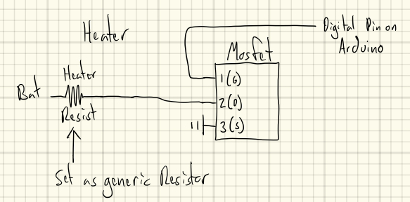
If you choose to use a heater, we will use a generic MOSFET, using the wiring diagram here. In this diagram, the MOSFET has pins 1 - G, 2 - D, and 3 - S. You can use a generic resistor to represent the heater, since it will just be soldered into place.
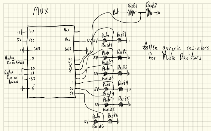
- If you use the photo-cells or a thermistor, you can use generic resistors, since these will be soldered with wires, so the connection type doesn’t really matter much. Both a photo-cell and a thermistor act as resistors, so you will be creating a voltage divider circuit, with a resistor in series with the photo-cell/thermistor, with the analog line coming off the wire in between the resistor and photo-cell/thermistor.
Procedure: Starting Your Design and Creating A Schematic
-
Download the updated “Final Project Library” folder from the link above.
-
Open KiCad on your computer. Navigate to File -> New Project…
-
The “Folder” field allows you to choose where this folder is created. You are going to zip this folder and share it with others. The folder should have your team number in it. Make sure to select the “create a new folder” option when naming and creating your project.
-
Name your project with your team number and an appropriate name (e.g., Team05_Project_PCB_V1.0), and click “Save”.
-
In your computer’s file directory, find the location of the new folder you just made. Inside of this folder, create another folder called “Libraries” and drag the Symbols, Footprints, and 3D Models libraries you just downloaded to this location.
-
On the open landing page for KiCad (where it shows the project directory), select “Preferences” > “Manage Symbol Libraries”. Open “Project Specific Libraries” and then select the folder icon on the bottom left (between a + icon and an up arrow). Navigate to your new “Libraries” folder, then to “Symbols”, and then select all of the .kicad_sym files shown there. Click open. You should now see all of the components loaded into this window with proper names. Click OK. You may be greeted with an error relating to other components, if it isn’t related to a component we are using for this project, feel free to click through the warning and move on.
-
Similarly, on the main landing page again, select “Preferences” > “Manage Footprint Libraries”. Same as before, click the folder icon on the bottom left, navigate to “Libraries” then “Footprints”, and then select all of the folders inside of this location. Yes, they should all be folders you are selecting this time, and they all end in .pretty. Click OK and navigate out of this window.
-
You should be able to click on the “Schematic Editor” and start making your schematic. Some notes:
-
Watch the youtube video to figure some things out.
-
You may need to manually link a footprint to a schematic symbol. To do that, use the Tools -> Assign Footprints menu. Make sure that you have added the footprint libraries.
-
Change the labels on things to make sense and so you can recognize them when they are dropped into the PCB. For example, if you have an LED and a resistor on the 5V line, call the LED “LED5V” and the resistor “R5V”. This should help a lot when you make the PCB.
-
Use nets for power (+5V, +3.3V, GND), but use wires for all other connections. This will make it much easier to find issues with the schematic.
-
That’s a lot to keep in mind. The path to success involves moving slowly and methodically through each component, writing out your schematic on paper beforehand, staying organized, and asking questions. If you’re confused, please ask. When you’ve finished your schematic, ask another team to take a look at your schematic. They can offer advice about any issues you may have. Then, ask an IA to check it off and verify that it is correct. Once they mark it off, you can move on to creating the PCB. It is in your best interest to have a clean and accurate schematic before moving forward. Even minor changes on the schematic can require substantial changes on your PCB to accommodate.
It is a good idea to design your schematic and then save everything. Make sure that you can quit out of KiCad and reopen the schematic. If, for some reason, you need to stop working on this, the end of the schematic creation is a good place to pause.
PCB
Background
The PCB is designed as a separate document with the extension .kicad_pcb. We can create a new PCB document and correlate it to our schematic. This will import all the components to the PCB document. Then, just as in the schematic document, we can manually place each footprint. As before, the footprints will be provided via a custom library we have prepared for you.
Note the white lines that connect each of the footprints in Figure 3. These represent which pins on each part should be connected via traces. This should be done manually, similar to how wires were drawn in the schematic. One notable difference is that physical traces should not be drawn at right angles; instead, they should be at obtuse angles. This is to minimize field leakage and reflection at corners.
Procedure: Designing the PCB
You can switch to the PCB editor in a couple of ways, such as pushing the “Switch to PCB Editor” button, which should be the right-most button on the top of the schematic editor.
You can then bring in changes from your schematic by clicking Tools -> Update PCB from Schematic… This will open a window with a lot of text while it imports information. It will tell you if there are warnings or errors. If there are errors, you need to fix them. For example, if something doesn’t have a footprint, it will give you an error. Go back to the schematic and fix any errors that you have. You may need to manually assign footprints.
Once you get to the PCB window, you will have a big cluster of components that you can drop towards the center of the layout window. You should be able to move each of the components around by clicking on part of the component (not the text labels, which you can move independently of the component) and moving it. You can rotate the component by pressing “R”. All components will show up on the top layer (the red layer).
KiCad uses layers, both on the PCB and in the software. On the PCB, there is the top layer (red) and the bottom layer (blue). In the software, these layers show up on the right side of KiCad as a list. The top two are “F.Cu”, which is the top layer of the PCB, and “B.Cu”, which is the bottom layer of the PCB. You can toggle back and forth between putting things on the top layer and bottom layer by clicking on which layer you would like to be active.
Another key layer that we care about is the “Edge.Cuts” layer. This allows us to size the PCB. You can select this layer and draw a box around all of the PCB components. The box should be (maximum) 100 mm x 100 mm in size. Once you draw this box, you can always make it smaller by switching back to the “Edge.Cuts” layer, and adjusting the size of the box.
Layout your components neatly on the board. Be sure to place your Arduino and data logger in such a way that you do not obstruct the port for the uploading cable or the SD card opening.
Place capacitors very close to the component that they are assigned to. The point of the capacitor is to decrease high-frequency noise. If you have too much wire between the capacitor and the component, the wire can act as an antenna and get high-frequency noise back into it. This is why we have so many capacitors on the board.
The light-cyan lines indicate which vias and pads should be connected to each other. Some of the lines are “unique”, such as an analog pin on the accelerometer going to an analog pin on the Arduino. Some of them are not unique, such as the 5V pin on the GPS connected to any other 5V pin. The cyan lines for non-unique pins will jump around as you move the component, since the lines connect the closest component that is on the same “rail”. There are a lot of ground pins, so the cyan lines for these will keep jumping around a lot.
Rotate components so that the cyan lines don’t cross each other as much (it is impossible for them to not really touch).
Don’t bother routing the ground pins at this point, since we will draw a ground pour at the end!
You can place routes on both the top and bottom layers. Any thru-hole component can be connected together on the bottom or top layer. Any surface-mount component will need a via next to it with a wire to connect to the other layer. You can switch to routing on the other layer by clicking on the other layer in the list of layers. If you are routing and the wire is blue, you are on the bottom layer; if it is red, you are on the top layer. Vias connect the layers together.
Before we trace, we need to set some design rules. To edit a design rule, go to File -> Board Setup -> Design Rules.
- Enter the value (and units) that is specified and click OK
- All below are minimum values
- 0.25 mm minimum clearance
- 0.15 mm trace width
- 0.25 mm copper to hole clearance
- 0.3 mm min through hole size
- 0.45 mm hole to hole clearance
- 0.15 mm annular width
- 1 mm copper to edge clearance
- Predefined sizes
- Tracks - 0.4 mm and 0.5 mm
- (0.5 mm traces will be used for power)
- Vias - Diameter 0.6 mm, Hole 0.3 mm
- Tracks - 0.4 mm and 0.5 mm
Make sure when you are placing traces or vias, that you are selecting these predefined sizes. (I know the video doesn’t go over this). Here’s what that looks like
To draw a wire on the PCB, it is called “routing”, so select Route -> Route Single Track (or just press ‘X’). You can now connect things together. When routing, all traces should default to 0.4 mm or 0.5 mm if you implemented the design rules correctly. For the power connections to the GPS, Arduino, and SD card reader, make sure to use 0.5 mm tracks in order to compensate for the increased current flow through them. For the heater (if you are using a heater), use 0.8 mm traces. You can select an existing trace and edit the width in Properties. All other traces can be 0.4 mm.
AGAIN, Don’t bother routing the ground pins at this point, since we will draw a ground pour at the end!
You can place routes on both the top and bottom layers. Any thru-hole component can be connected together on the bottom or top layer. Any surface-mount component will need a via next to it with a wire to connect to the other layer. You can switch to routing on the other layer by clicking on the other layer in the list of layers. If you are routing and the wire is blue, you are on the bottom layer, if it is red, you are on the top layer. Vias connect the layers together.
Recall from lecture that your board contains two copper layers. These layers are referred to as the top and bottom layers, and are colored red and blue. You can route traces on either side of the board. You need to exit trace placement, then switch layers (by clicking on the layer that you want), then go back to placing traces. The layers that are important to use are listed below:
- Top Layer - Top of the board electrical connections (F.cu)
- Bottom Layer - Bottom of the board for electrical connections (B.cu)
- F.Silkscreen - Your silkscreen for the top layer; edit labels and add any text
- B.Silkscreen - Your silkscreen for the bottom layer; edit labels and add any text
When routing, you may notice obvious conflicts (lots of traces need to cross). You can play with the design by rotating components, moving components, or rearranging your components to ease these conflicts. You may have to do this a few times, so when you place a trace the first time, don’t think of it as the final time - think of this as a sketch that you are refining as you go. It is OK (and expected) to delete traces, move things, and retrace. Use both layers of the board to trace. Remember that through-hole components are connected on both sides of the board, so you can trace on either side.
You can also use Vias to have a trace go from the top layer to the bottom layer or bottom to the top layer. You can use this technique when you have to cross another trace. Most trace crossings can be avoided with some thinking about placement of components, orientation of the different components, or tracing using different routes. Routes should not be too long, though! Don’t have super long traces to avoid crossing.
When placing a via, you may have to assign it to a net. If you just randomly place a via, KiCad probably won’t allow you to randomly connect a wire to it. If you need to connect something to it, look at one of the locations where you are connecting it from/to. There will be tiny letters that say something like “Net - (A1-A3)” or similar. You can double click on the via, which brings up Properties. Uncheck “Automatically update via nets” and assign it to the net that you want to connect it to. If you did it right, KiCad will let you connect the via to the component.
You can place text labels or indicators (Place -> Text) on your PCB to help you remember things. Because LEDs are directional, you may want to indicate which sides are positive by adding a “+” label near the high-voltage side. Labels are good. Note that this is different from “Net labels”. You MUST label your board with your team number and name, as well as the date and your names if you would like.
A very common industry standard is to use a filled zone so you don’t have to run a lot of lines to ground and/or power. A zone that is usually used is a GND pour over the entire bottom layer, which is how we will use this. If you add a filled zone for the GND net on the entire bottom layer, then all components that have GND pins in the bottom layer will be connected and you do not need traces to connect them. To do this:
-
Make sure you have selected the layer you want to place your polygon pour (F.cu or B.cu)
-
Use the Add Filled Zone tool from the right toolbar (or Place -> Add Filled Zone).
-
Click one corner of the PCB to start, it does not matter which corner.
-
Under Net Options, select the net you’d like to connect to
-
The net should have been defined in your schematic (i.e. GND, 5V, BAT, 3.3V)
-
Under layer, select the layer you’d like this pour to be on
-
Click OK, then click around until you are satisfied with the shape, then press Esc to finish the outline. Use the Fill All Zones tool (or the toolbar button) to fill the zone.
You can adjust dimensions of the zone later if needed. Every single time you adjust components from now on, you’ll need to refill the zone afterward (this is why you may want to wait until the end to do the zone).
You can use vias to connect your Surface Mount Components to the Ground pour, or do a ground pour on both the top and bottom layer. That will cover the surface mount components.
Finally, we have a completed board. In KiCad, you can view the 3D model of the PCB by clicking View -> 3D Viewer (like Figure 4) before moving on to the final stage: Design Rule Check.
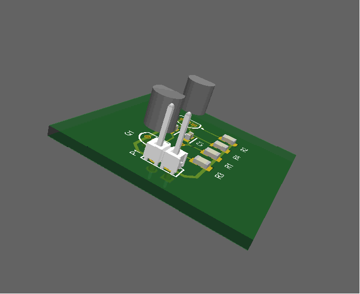
Figure 4: Completed PCB
DRC
The DRC, or Design Rule Check, is a way to check the validity of your PCB with respect to the design rules we create. More on this in the procedure.
Procedure: Design Rules Check
- Ensure you are achieving mechanical specs set by the manufacturer based on the fidelity of their equipment
- To edit a design rule, go to File -> Board Setup -> Design Rules.
- Enter the value (and units) that is specified and click OK
- Once you have all rules edited per the guidelines, click Inspect -> Design Rules Checker to run the DRC
- Click on Run Design Rule Check on bottom left
- You need ZERO errors and warnings before you can manufacture the design, we will require it as part of your final submission (unless it is a silkscreen error, those are just aesthetics)
- You will also need some pre-defined sizes. You did this in step 1.
Final Deliverable
Each team must upload a single zip file containing all project files, project libraries, and a screenshot showing all DRCs passed to this designated Google Drive folder (linked in the Canvas assignment) by the date and time specified on the Canvas assignment.
Each student will peer review three PCBs with rubrics provided on Canvas.
The zip file must:
- Contain all information so that another person can unzip the file, open KiCad, and see your schematic and PCB. (Make sure to include the ‘Libraries’ folder, formatted as required above).
- Be named with the following template: teamXX_PCB_initial.zip or teamXX_PCB_final.zip, where XX is your team number expressed as two digits (e.g., 01, 02, 10, 11, etc.)
Peer Review
After the lab, every student will be required to peer review the PCBs of three other teams.
There is a Canvas assignment as well as a Google Form that must be filled out for each review.
Peer Review and Final Submission
- Submit your error-free DRC screenshot and all project files to the designated Google Drive folder by the assignment deadline discussed in class and posted on the Canvas assignment.
- Peer review three other teams’ PCBs using provided rubrics by the date and time stated in the Canvas assignment.
Remember, accuracy and collaboration are essential. Reach out to IAs, Professor Ridley, or the #lab-help channel on Slack for assistance if needed. Good luck with your PCB design!